半导体基础知识(1):材料和器件
写在前面
2020年5月26晚记,昨天刚毕业答辩结束,即使通过了,由于后面还有很大概率继续抽取校盲,论文还是要添加以及修改。
在仿真的过程中,由于电脑性能太差,以及MATLAB仿真时间过长,这个等待的过程中,闲来无事,不如看看文章,总体而言,英文文章质量更佳,这里不如翻译一些基础内容来消遣等待的时光。
译文源链接:Semiconductor Basics: Materials and Devices
原文是一个视频,但是由于是国外网站上的视频(YouTube),因此加载是个问题,好在有正文。
该视频教程讨论了基本的半导体概念,并介绍了我们用来将半导体变成有用的电子组件的技术。
在本视频教程中,我们将讨论半导体材料以及它们如何成为有用的电子组件,即通过半导体掺杂。
正文
什么是半导体?
“半导体”一词已经与先进的电子技术联系在一起,后者在二十世纪下半叶迅速改变了人类的生活。 但是,就其本身而言,半导体并不十分引人注目:它只是一种具有中等导电性的材料-也就是说,它的导电性比导体小,但比绝缘体大。
热能使价电子脱离半导体的晶格结构,从而变成“自由”电子。 这些移动电子是可以在施加的电场的影响下移动的负电荷,这些自由电子留下的空穴起移动正电荷的作用。 电子和空穴都参与半导体电流,并且半导体的电学性质受材料中存在的自由电子和空穴的数量影响。
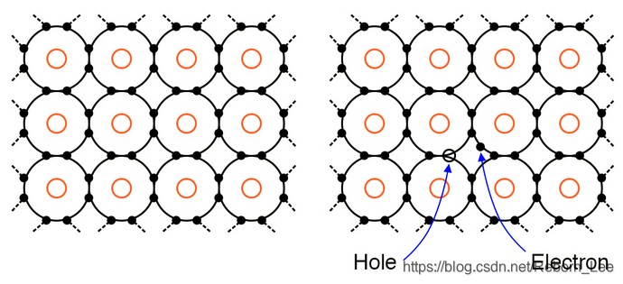
左侧的图表示半导体的规则晶格,而右侧的图包括电子-空穴对。
普通的未经修饰的半导体无法提供有用的电气功能。 将半导体转变为技术革命手段的第一步称为掺杂。
半导体掺杂
我们可以通过将其他材料注入晶格结构来控制半导体中载流子的数量。 更具体地说,我们注入具有不同价电子数量的材料。
假设我们的半导体是硅(Si),它是IV组元素,因此具有四个价电子。 如上图所示,硅原子通过共价键结合成规则的晶格结构。 诸如磷(P)之类的V组元素具有五个价电子,如果我们将磷注入硅中,每个注入的原子都会向半导体的晶格中引入一个自由电子:
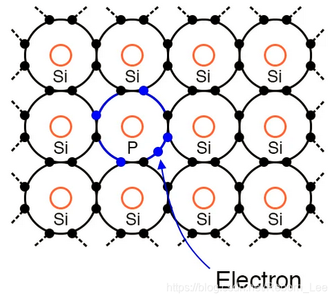
用V族元素掺杂会引入自由电子。
在这种情况下,磷起掺杂剂的作用,硅成为n型半导体:它通过掺杂获得了额外的自由电子,当施加电场时,电流将主要归因于具有负电荷的电子 。 因此,在n型半导体中,电子是多数载流子,空穴是少数载流子。
另一方面,如果我们用III族元素(例如硼(B))掺杂,则每个掺杂原子都会引入一个额外的空穴。 这将硅变成p型半导体:空穴的数量超过了自由电子的数量,电流的流动将主要归因于正电荷的运动。 因此,在p型半导体中,空穴是多数载流子,电子是少数载流子。
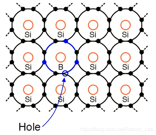
用III族元素掺杂会引入空穴。
注入元素并不是掺杂过程中唯一的变量。 我们还可以控制掺杂剂的浓度,从而影响半导体的电学行为。 当半导体包含相对较高浓度的掺杂原子时,我们称其为重掺杂。 如果它包含相对较低浓度的掺杂剂原子,则它是轻度掺杂的。 例如,将在以后的教程中讨论的场效应晶体管将重掺杂硅用作源极和漏极区域。
结论
如果目标是制造有用的电子组件,那么掺杂材料本身并没有比原始半导体更好。 但是,当我们将n型半导体与p型半导体相邻放置时,一切都会改变。 此结构称为pn结,是下一个教程的主题。
原文附录
This video tutorial discusses basic semiconductor concepts and introduces the techniques that we use to turn semiconductors into useful electronic components.
In this video tutorial, we’ll discuss semiconductor materials and how they become useful electronic components—namely, through semiconductor doping.
What Is a Semiconductor?
The word “semiconductor” has become associated with the sophisticated electronic technology that rapidly transformed human life during the second half of the twentieth century. However, on its own, a semiconductor is rather unremarkable: it is simply a material that exhibits mediocre conductivity—that is, it’s less conductive than a conductor but more conductive than an insulator.
Thermal energy causes valence electrons to break out of a semiconductor’s lattice structure and thereby become “free” electrons. These mobile electrons are negative charges that can move under the influence of an applied electric field, and the holes left behind by these free electrons function as mobile positive charges. Both electrons and holes participate in semiconductor current flow, and the electrical properties of a semiconductor are affected by the number of free electrons and holes that are present in the material.
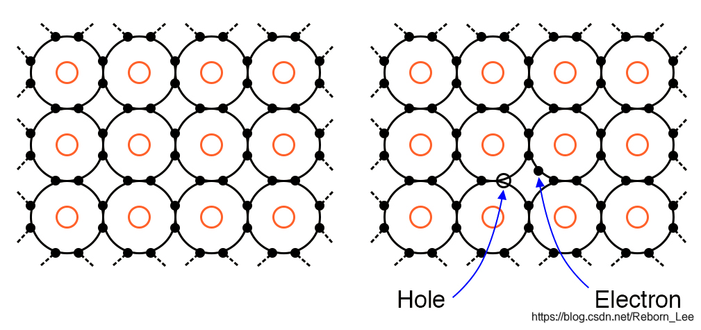
The diagram on the left represents the regular crystal lattice of a semiconductor, and the diagram on the right includes an electron-hole pair.
Ordinary unmodified semiconductors don’t offer much in the way of useful electrical functionality. The first step in turning a semiconductor into a means of technological revolution is called doping.
Semiconductor Doping
We can control the quantity of charge carriers in a semiconductor by injecting other materials into the lattice structure. More specifically, we inject materials that have a different number of valence electrons.
Let’s say that our semiconductor is silicon (Si), which is a group IV element and thus has four valence electrons. As shown in the previous diagram, silicon atoms combine via covalent bonding into a regular lattice structure. A group V element such as phosphorus § has five valence electrons, and if we inject phosphorus into the silicon, each injected atom will introduce a free electron into the semiconductor’s crystal lattice:
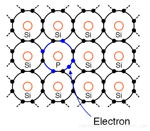
Doping with a group V element introduces free electrons.
In this situation, phosphorus functions as a dopant and the silicon becomes an n-type semiconductor: it has received additional free electrons through doping, and when an electric field is applied, current flow will be due primarily to electrons, which have a negative charge. Thus, in an n-type semiconductor, electrons are the majority carriers and holes are the minority carriers.
If, on the other hand, we dope with a group III element such as boron (B), each doping atom will introduce an additional hole. This turns the silicon into a p-type semiconductor: holes outnumber free electrons, and current flow will be due primarily to the movement of positive charges. Thus, in a p-type semiconductor, holes are the majority carriers and electrons are the minority carriers.
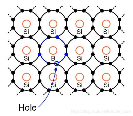
Doping with a group III element introduces holes.
The injected element is not the only variable in doping procedures. We can also control the dopant concentration, which in turn influences the electrical behavior of a semiconductor. When a semiconductor contains a relatively high concentration of dopant atoms, we call it heavily doped. If it contains a relatively low concentration of dopant atoms, it is lightly doped. For example, field-effect transistors, which will be discussed in a future tutorial, use heavily doped silicon for the source and drain regions.
Conclusion
If the goal is to create useful electronic components, a doped material by itself is not really any better than the original semiconductor. However, when we place an n-type semiconductor adjacent to a p-type semiconductor, everything changes. This structure, called a pn junction, is the subject of the next tutorial.
文章来源: reborn.blog.csdn.net,作者:李锐博恩,版权归原作者所有,如需转载,请联系作者。
原文链接:reborn.blog.csdn.net/article/details/106346567
- 点赞
- 收藏
- 关注作者


评论(0)