半导体基础知识(2):PN结二极管和二极管特性
写在前面
从第一篇文章开始:半导体基础知识(1):材料和器件,觉得挺好,于是决定翻译第二篇,有缘看到就进行下去。
上篇最后预留了这样一句话:
如果目标是制造有用的电子组件,那么掺杂材料本身并没有比原始半导体更好。 但是,当我们将n型半导体与p型半导体相邻放置时,一切都会改变。 此结构称为pn结,是下一个教程的主题。
这恰好呼应地也是这篇文章,单纯的掺杂可没什么好说的,要对目标有用,才是掺杂的目的。我们要用掺杂的半导体材料做成有用的电子器件,就需要将掺杂后的n型半导体和p型半导体相邻放置!
原文链接:The PN Junction Diode and Diode Characteristics
该篇教程探讨了通过将n型半导体材料与p型半导体材料接触而形成的电子结构的物理和电气行为。
正文
半导体组件(不仅是二极管和晶体管,而且是不常见的设备,例如TRIAC和可控硅的开关)是通过组合n型和p型半导体而构成的。 因此,重要的是要了解在n型和p型材料之间的界面处会发生什么。 我们将此接口称为pn结。
pn结和半导体二极管
当我们专注于半导体操作的物理学时,我们使用术语pn结; 当我们专注于电路设计时,我们使用二极管一词。 但是它们本质上是同一回事:基本的半导体二极管是连接有导电端子的pn结。 首先让我们看一下图表,然后我们将简要探讨这个极为重要的电路元件的行为。

左边的实心圆是空穴,右边的实心圆是电子。耗尽区由与来自n型半导体的自由电子重新结合的空穴(这些重新结合的空穴由带圆圈的负号表示)和与来自p型半导体的空穴重新结合的电子(以圆圈正号表示)组成。该复合导致耗尽区的p型部分带负电,并且耗尽区的n型部分带正电。
在p型和n型材料的接合处电荷的分离会导致电位差,称为接触电位。在硅pn结二极管中,接触电势约为0.6V。如上图所示,该电势的极性与我们预期的相反:在n型侧为正,而在p型侧为负。
电流可以通过扩散流过结-由于结两部分的电荷载流子浓度不同,一些来自p型材料的空穴将扩散到n型材料中,而一些来自n型电子型材料将扩散到p型材料中。但是,几乎没有电流流过,因为接触电势对该扩散电流起阻挡作用。此时,我们将开始使用术语势垒电压代替接触电势。
正向和反向偏置
如果我们将二极管连接到电池上,使得电池的电压与势垒电压具有相同的极性,则结点将被反向偏置。 由于我们正在增加势垒电压,因此扩散电流进一步受到阻碍。

施加反向偏置电压会使结的耗尽区变宽。
另一方面,如果我们将电池的正极连接到二极管的p型侧,而负极将连接到n型侧,则我们正在降低势垒电压,从而促进电荷载流子在结上的扩散。 但是,在我们克服势垒电压并完全耗尽耗尽区之前,电流量将保持相当低的水平。 这在施加的电压等于势垒电压时发生,并且在这些正向偏置条件下,电流开始自由流过二极管。

二极管作为电路组件
前面的讨论揭示了产生硅二极管电行为的两个最突出特征的基本物理过程。
首先,当以反向偏压极性施加电压时,pn结阻止电流流动,而当以正偏压极性施加电压时,pn结允许电流流动。 这就是为什么二极管可以用作电流的单向阀的原因。
其次,当施加的正向偏置电压接近势垒电压时,流过二极管的电流呈指数增长。 这种指数电压-电流关系使正向偏置二极管的电压降保持相当稳定,如下图所示。

二极管的工作量可以近似为一个恒定的电压降,因为很小的电压增加对应于很大的电流增加。
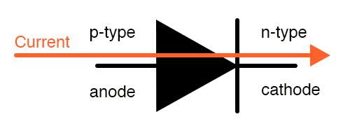
下图阐明了二极管的物理结构,其电路符号以及我们用于其两个端子的名称之间的关系。 施加正向偏置电压会使电流沿蓝色箭头方向流动。

结论
现在,我们已经介绍了半导体功能的基本方面,并且在下一个教程中,我们将探讨晶体管,这是迎来电子时代的半导体组件。
原文附录
Semiconductor components—not only diodes and transistors but also less-common devices such as TRIACs and silicon-controlled switches—are constructed by combining n-type and p-type semiconductors. Thus, it is important to understand what occurs at the interface between n-type and p-type materials; we call this interface the pn junction.
The pn Junction and the Semiconductor Diode
When we’re focusing on the physics of semiconductor operation, we use the term pn junction; when we’re focusing on circuit design, we use the term diode. But they’re essentially the same thing: a basic semiconductor diode is a pn junction with conductive terminals attached. First let’s look at a diagram, and then we’ll briefly explore the behavior of this extremely important circuit element.

The unfilled circles on the left are holes, and the solid circles on the right are electrons. The depletion region consists of holes that have recombined with free electrons from the n-type semiconductor (these recombined holes are represented by circled negative signs) and electrons that have recombined with holes from the p-type semiconductor (represented by circled positive signs). This recombination causes the p-type portion of the depletion region to be negatively charged and the n-type portion of the depletion region to be positively charged.
The separation of charge at the junction of the p-type and n-type materials results in a potential difference called the contact potential. In a silicon pn-junction diode, the contact potential is about 0.6 V. As you can see in the previous diagram, the polarity of this potential is the opposite of what we might expect: it is positive on the n-type side and negative on the p-type side.
Current can flow through the junction by means of diffusion—because of differences in charge-carrier concentrations in the two portions of the junction, some holes from the p-type material will diffuse into the n-type material, and some electrons from the n-type material will diffuse into the p-type material. However, very little current flows because the contact potential functions as a barrier to this diffusion current. At this point we will begin using the term barrier voltage instead of contact potential.
Forward and Reverse Bias
If we connect the diode to a battery such that the battery’s voltage has the same polarity as the barrier voltage, the junction is reverse-biased. Diffusion current is further impeded because we are increasing the barrier voltage.

Applying a reverse-bias voltage widens the junction’s depletion region.
If, on the other hand, we connect the battery’s positive terminal to the p-type side of the diode and the negative terminal to the n-type side, we are decreasing the barrier voltage and thereby facilitating charge-carrier diffusion across the junction. However, the amount of current will remain quite low until we overcome the barrier voltage and fully collapse the depletion region. This occurs when the applied voltage is equal to the barrier voltage, and under these forward-biased conditions, current begins to flow freely through the diode.

Diodes as Circuit Components
The preceding discussion reveals the underlying physical processes that produce the two most prominent characteristics of a silicon diode’s electrical behavior.
First, a pn junction resists current flow when voltage is applied in reverse-bias polarity and allows current flow when voltage is applied in forward-bias polarity. This is why a diode can function as a one-way valve for electric current.
Second, current flow through a diode increases exponentially as the applied forward-bias voltage approaches the barrier voltage. This exponential voltage–current relationship causes the voltage drop of a forward-biased diode to remain fairly stable, as conveyed by the following plot.

Diode operation can be approximated as a constant voltage drop because large increases in current correspond to very small increases in voltage.
The following diagram clarifies the relationship between the physical structure of a diode, its circuit symbol, and the names that we use for its two terminals. Applying a forward-bias voltage causes current to flow in the direction of the blue arrow.

Conclusion
We have now covered foundational aspects of semiconductor functionality, and in the next tutorial we’ll explore the transistor, which is the semiconductor component that ushered in the electronic age.
文章来源: reborn.blog.csdn.net,作者:李锐博恩,版权归原作者所有,如需转载,请联系作者。
原文链接:reborn.blog.csdn.net/article/details/106360265
- 点赞
- 收藏
- 关注作者


评论(0)