Verilog设计实例(2)一步一步实现一个多功能通用计数器

写在前面
正文
多功能计数器,英文名为:Versatile Counter;所谓多功能,这里包括二进制计数,格雷码计数以及线性反馈移位寄存器(LFSR)三种,本文通过从普通的计数器开始,也就是单个功能的计数器开始,一步一步过渡到多功能计数器。
作为对以下相关博文的延伸练习:
Verilog设计实例(1)线性反馈移位寄存器(LFSR)
FPGA设计心得(8)Verilog中的编译预处理语句
普通的二进制计数器
这个作为开头,不必多说,计数就完事了。
电路设计
设计文件:
`timescale 1ns/1ps
//
// Engineer: Reborn Lee
// Module Name: binary counter
// Additional Comments:
//
//
module binary_counter#(parameter N_BITS = 4)(
	input i_clk,
	input i_rst,
	output [N_BITS - 1 : 0] o_cnt,
	output o_cnt_done
	);

	reg [N_BITS - 1 : 0] bin_cnt = 0;
	always@(posedge i_clk) begin
		if(i_rst) begin bin_cnt <= 0;
		end
		else begin bin_cnt <= bin_cnt + 1;
		end
	end

	assign o_cnt_done = (bin_cnt == 0)? 1:0;
	assign o_cnt = bin_cnt;


endmodule
- 1
- 2
- 3
- 4
- 5
- 6
- 7
- 8
- 9
- 10
- 11
- 12
- 13
- 14
- 15
- 16
- 17
- 18
- 19
- 20
- 21
- 22
- 23
- 24
- 25
- 26
- 27
- 28
- 29
行为仿真
tb文件:
`timescale 1ns/1ps
module bin_cnt_tb;

	parameter N_BITS = 4;
	reg i_clk;
	reg i_rst;
	wire [N_BITS - 1 : 0] o_cnt;
	wire o_cnt_done;

	initial begin
		i_clk = 0;
		forever begin # 2 i_clk = ~ i_clk;
		end
	end

	initial begin
		i_rst = 1; # 8
		i_rst = 0;

	end

	binary_counter #(.N_BITS(N_BITS))
	inst_bin_cnt(
		.i_rst(i_rst),
		.i_clk(i_clk),
		.o_cnt(o_cnt),
		.o_cnt_done(o_cnt_done)
		);
endmodule
- 1
- 2
- 3
- 4
- 5
- 6
- 7
- 8
- 9
- 10
- 11
- 12
- 13
- 14
- 15
- 16
- 17
- 18
- 19
- 20
- 21
- 22
- 23
- 24
- 25
- 26
- 27
- 28
- 29
- 30
- 31
- 32
仿真图:

普通的格雷码计数器
任意位宽的格雷码计数器,实现的方式通常是设计一个普通的二进制计数器,同时将计数结果转化为格雷码。
二进制与格雷码的转换方式,详情见:格雷码和二进制转换。
为了方便给出原理图:

伪代码描述为:
assign gray_value = binary_value ^ (binary_value>>1);
- 1
或者:
assign gray_cnt = { bin_cnt[N_BITS - 1], bin_cnt[N_BITS - 1 : 1]^bin_cnt[N_BITS - 2 : 0]};
- 1
电路设计
一种简单的设计方式为:
`timescale 1ns / 1ps
//
// Engineer: Reborn Lee
// Create Date: 2020/06/02 13:46:10
// Module Name: gray_counter
// Additional Comments: common gray counter
//
//


module gray_counter #(parameter N_BITS = 4)(
	input i_clk,
	input i_rst,
	output [N_BITS - 1 : 0] o_cnt,
	output o_cnt_done ); reg [N_BITS - 1 : 0] bin_cnt = 0;
	reg [N_BITS - 1 : 0] gray_cnt;
	always@(posedge i_clk) begin
		if(i_rst) begin bin_cnt <= 0; gray_cnt <= 0;
		end
		else begin bin_cnt <= bin_cnt + 1; // translate binary counter into  gray counter gray_cnt <= bin_cnt ^ bin_cnt >>> 1; //or // gray_cnt <= { bin_cnt[N_BITS - 1], bin_cnt[N_BITS - 1 : 1]^bin_cnt[N_BITS - 2 : 0]}; //or // for(int i = 0; i < N_BITS - 1; i = i + 1) begin // 	gray_cnt[i] <= bin_cnt[i+1]^bin_cnt[i]; // end // gray_cnt[N_BITS - 1] <= bin_cnt[N_BITS - 1]; end

	end

	assign o_cnt = gray_cnt;
	// or
	assign o_cnt_done = (gray_cnt == 0) ? 1 : 0; endmodule
- 1
- 2
- 3
- 4
- 5
- 6
- 7
- 8
- 9
- 10
- 11
- 12
- 13
- 14
- 15
- 16
- 17
- 18
- 19
- 20
- 21
- 22
- 23
- 24
- 25
- 26
- 27
- 28
- 29
- 30
- 31
- 32
- 33
- 34
- 35
- 36
- 37
- 38
- 39
- 40
- 41
- 42
- 43
- 44
- 45
- 46
- 47
- 48
- 49
- 50
- 51
- 52
注释部分解释:
for(int i = 0; i < N_BITS - 1; i = i + 1) begin gray_cnt[i] <= bin_cnt[i+1]^bin_cnt[i]; end gray_cnt[N_BITS - 1] <= bin_cnt[N_BITS - 1];
- 1
- 2
- 3
- 4
以及:
gray_cnt <= { bin_cnt[N_BITS - 1], bin_cnt[N_BITS - 1 : 1]^bin_cnt[N_BITS - 2 : 0]};
- 1
均在always块内,因此使用非阻塞赋值。
又和二进制计数在一起always内,且紧邻分布,因此计数相较于二进制慢一拍,但毫无影响(不影响计数总数)。
注: 三种二进制转换为格雷码的实现原理一致,效果等价。
行为仿真
TestBench设计:
`timescale 1ns/1ps
module gray_cnt_tb;

	parameter N_BITS = 4;
	reg i_clk;
	reg i_rst;
	wire [N_BITS - 1 : 0] o_cnt;
	wire o_cnt_done;

	initial begin
		i_clk = 0;
		forever begin # 2 i_clk = ~ i_clk;
		end
	end

	initial begin
		i_rst = 1; # 8
		i_rst = 0;

	end

	gray_counter #(.N_BITS(N_BITS))
	inst_gray_cnt(
		.i_rst(i_rst),
		.i_clk(i_clk),
		.o_cnt(o_cnt),
		.o_cnt_done(o_cnt_done)
		);
endmodule
- 1
- 2
- 3
- 4
- 5
- 6
- 7
- 8
- 9
- 10
- 11
- 12
- 13
- 14
- 15
- 16
- 17
- 18
- 19
- 20
- 21
- 22
- 23
- 24
- 25
- 26
- 27
- 28
- 29
- 30
- 31
- 32
行为仿真波形:
局部放大:
LFSR
这个请参考上篇博文,单独做了一篇博客:
Verilog设计实例(1)线性反馈移位寄存器(LFSR)
为了方便不跳转另外一个链接,这里给出设计:
电路设计
`timescale 1ns / 1ps
//
// Company:
// Engineer: Reborn Lee
// Create Date: 2020/06/01 12:50:38
// Design Name:
// Module Name: lfsr
// Revision 0.01 - File Created
// Additional Comments:
//
//


module lfsr #(parameter NUM_BITS = 3)( input i_Clk, input i_Enable, // data valid input i_Seed_DV, // Optional Seed Value input [NUM_BITS-1:0] i_Seed_Data, output [NUM_BITS-1:0] o_LFSR_Data, output o_LFSR_Done ); // internal variables
  reg [NUM_BITS:1] r_LFSR = 0;
  reg r_XNOR; // Purpose: Load up LFSR with Seed if Data Valid (DV) pulse is detected.
  // Othewise just run LFSR when enabled. always @(posedge i_Clk) begin if (i_Enable == 1'b1) begin if (i_Seed_DV == 1'b1) r_LFSR <= i_Seed_Data; else r_LFSR <= {r_LFSR[NUM_BITS-1:1],r_XNOR}; //left right end end

// Create Feedback Polynomials.  Based on Application Note:
  // http://www.xilinx.com/support/documentation/application_notes/xapp052.pdf always @(*) begin case (NUM_BITS) 3: begin r_XNOR = r_LFSR[3] ^~ r_LFSR[2]; end 4: begin r_XNOR = r_LFSR[4] ^~ r_LFSR[3]; end 5: begin r_XNOR = r_LFSR[5] ^~ r_LFSR[3]; end 6: begin r_XNOR = r_LFSR[6] ^~ r_LFSR[5]; end 7: begin r_XNOR = r_LFSR[7] ^~ r_LFSR[6]; end 8: begin r_XNOR = r_LFSR[8] ^~ r_LFSR[6] ^~ r_LFSR[5] ^~ r_LFSR[4]; end 9: begin r_XNOR = r_LFSR[9] ^~ r_LFSR[5]; end 10: begin r_XNOR = r_LFSR[10] ^~ r_LFSR[7]; end 11: begin r_XNOR = r_LFSR[11] ^~ r_LFSR[9]; end 12: begin r_XNOR = r_LFSR[12] ^~ r_LFSR[6] ^~ r_LFSR[4] ^~ r_LFSR[1]; end 13: begin r_XNOR = r_LFSR[13] ^~ r_LFSR[4] ^~ r_LFSR[3] ^~ r_LFSR[1]; end 14: begin r_XNOR = r_LFSR[14] ^~ r_LFSR[5] ^~ r_LFSR[3] ^~ r_LFSR[1]; end 15: begin r_XNOR = r_LFSR[15] ^~ r_LFSR[14]; end 16: begin r_XNOR = r_LFSR[16] ^~ r_LFSR[15] ^~ r_LFSR[13] ^~ r_LFSR[4]; end 17: begin r_XNOR = r_LFSR[17] ^~ r_LFSR[14]; end 18: begin r_XNOR = r_LFSR[18] ^~ r_LFSR[11]; end 19: begin r_XNOR = r_LFSR[19] ^~ r_LFSR[6] ^~ r_LFSR[2] ^~ r_LFSR[1]; end 20: begin r_XNOR = r_LFSR[20] ^~ r_LFSR[17]; end 21: begin r_XNOR = r_LFSR[21] ^~ r_LFSR[19]; end 22: begin r_XNOR = r_LFSR[22] ^~ r_LFSR[21]; end 23: begin r_XNOR = r_LFSR[23] ^~ r_LFSR[18]; end 24: begin r_XNOR = r_LFSR[24] ^~ r_LFSR[23] ^~ r_LFSR[22] ^~ r_LFSR[17]; end 25: begin r_XNOR = r_LFSR[25] ^~ r_LFSR[22]; end 26: begin r_XNOR = r_LFSR[26] ^~ r_LFSR[6] ^~ r_LFSR[2] ^~ r_LFSR[1]; end 27: begin r_XNOR = r_LFSR[27] ^~ r_LFSR[5] ^~ r_LFSR[2] ^~ r_LFSR[1]; end 28: begin r_XNOR = r_LFSR[28] ^~ r_LFSR[25]; end 29: begin r_XNOR = r_LFSR[29] ^~ r_LFSR[27]; end 30: begin r_XNOR = r_LFSR[30] ^~ r_LFSR[6] ^~ r_LFSR[4] ^~ r_LFSR[1]; end 31: begin r_XNOR = r_LFSR[31] ^~ r_LFSR[28]; end 32: begin r_XNOR = r_LFSR[32] ^~ r_LFSR[22] ^~ r_LFSR[2] ^~ r_LFSR[1]; end endcase // case (NUM_BITS) end // always @ (*) assign o_LFSR_Data = r_LFSR[NUM_BITS:1]; // Conditional Assignment (?)
 	assign o_LFSR_Done = (r_LFSR[NUM_BITS:1] == i_Seed_Data) ? 1'b1 : 1'b0;


endmodule
- 1
- 2
- 3
- 4
- 5
- 6
- 7
- 8
- 9
- 10
- 11
- 12
- 13
- 14
- 15
- 16
- 17
- 18
- 19
- 20
- 21
- 22
- 23
- 24
- 25
- 26
- 27
- 28
- 29
- 30
- 31
- 32
- 33
- 34
- 35
- 36
- 37
- 38
- 39
- 40
- 41
- 42
- 43
- 44
- 45
- 46
- 47
- 48
- 49
- 50
- 51
- 52
- 53
- 54
- 55
- 56
- 57
- 58
- 59
- 60
- 61
- 62
- 63
- 64
- 65
- 66
- 67
- 68
- 69
- 70
- 71
- 72
- 73
- 74
- 75
- 76
- 77
- 78
- 79
- 80
- 81
- 82
- 83
- 84
- 85
- 86
- 87
- 88
- 89
- 90
- 91
- 92
- 93
- 94
- 95
- 96
- 97
- 98
- 99
- 100
- 101
- 102
- 103
- 104
- 105
- 106
- 107
- 108
- 109
- 110
- 111
- 112
- 113
- 114
- 115
- 116
- 117
- 118
- 119
- 120
- 121
- 122
- 123
- 124
- 125
- 126
- 127
- 128
- 129
- 130
- 131
- 132
- 133
- 134
- 135
- 136
- 137
- 138
- 139
- 140
- 141
- 142
- 143
- 144
- 145
- 146
- 147
- 148
- 149
- 150
- 151
- 152
- 153
- 154
行为仿真
`timescale 1ns / 1ps
module lfsr_tb (); parameter c_NUM_BITS = 4; reg r_Clk = 1'b0; wire [c_NUM_BITS-1:0] w_LFSR_Data;
  wire w_LFSR_Done; lfsr #(.NUM_BITS(c_NUM_BITS)) LFSR_inst (.i_Clk(r_Clk), .i_Enable(1'b1), .i_Seed_DV(1'b0), .i_Seed_Data({c_NUM_BITS{1'b0}}), // Replication .o_LFSR_Data(w_LFSR_Data), .o_LFSR_Done(w_LFSR_Done) ); always @(*) #10 r_Clk <= ~r_Clk; endmodule // LFSR_TB
- 1
- 2
- 3
- 4
- 5
- 6
- 7
- 8
- 9
- 10
- 11
- 12
- 13
- 14
- 15
- 16
- 17
- 18
- 19
- 20
- 21
- 22
- 23
- 24
仿真波形:
多功能计数器
有了上面三种计数器的单独设计,下面该考虑组合起来了,是用什么样的方式组合?
用户可以选择,可以通过定义条件编译的方式,定义了某个宏就执行某种计数器,计数位宽可选择,通过参数化的方式实现。
电路设计
本设计用到了上面的三个模块,例化到本模块使用;
`timescale 1ns / 1ps
//
// Company:
// Engineer:
//
// Create Date: 2020/06/02 16:22:52
// Design Name:
// Module Name: versatile_counter
// Project Name:
// Target Devices:
// Tool Versions:
// Description:
//
// Dependencies:
//
// Revision:
// Revision 0.01 - File Created
// Additional Comments:
//
//

// `define LFSR_MACRO
`define GRAY
// `define BIN
module versatile_counter #(parameter N_BITS = 4)(
	input i_clk,
	input i_rst,
	output [N_BITS - 1 : 0] o_out,
	output o_out_done );

	`ifdef LFSR_MACRO

	lfsr #(.NUM_BITS(N_BITS)) LFSR_inst (.i_Clk(i_clk), .i_Enable(1'b1), .i_Seed_DV(1'b0), .i_Seed_Data({N_BITS{1'b0}}), // Replication .o_LFSR_Data(o_out), .o_LFSR_Done(o_out_done) ); `elsif GRAY

	gray_counter #(.N_BITS(N_BITS))
	inst_gray_cnt(
		.i_rst(i_rst),
		.i_clk(i_clk),
		.o_cnt(o_out),
		.o_cnt_done(o_out_done)
		); `else
	binary_counter #(.N_BITS(N_BITS))
	inst_bin_cnt(
		.i_rst(i_rst),
		.i_clk(i_clk),
		.o_cnt(o_out),
		.o_cnt_done(o_out_done)
		);

	`endif


endmodule
- 1
- 2
- 3
- 4
- 5
- 6
- 7
- 8
- 9
- 10
- 11
- 12
- 13
- 14
- 15
- 16
- 17
- 18
- 19
- 20
- 21
- 22
- 23
- 24
- 25
- 26
- 27
- 28
- 29
- 30
- 31
- 32
- 33
- 34
- 35
- 36
- 37
- 38
- 39
- 40
- 41
- 42
- 43
- 44
- 45
- 46
- 47
- 48
- 49
- 50
- 51
- 52
- 53
- 54
- 55
- 56
- 57
- 58
- 59
- 60
- 61
- 62
- 63
- 64
- 65
- 66
- 67
- 68
- 69
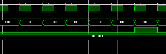
这里约定定义了宏GRAY,就是跑格雷码的代码,定义了宏BIN,就是跑二进制的代码,定义了LFSR_MACRO,就是跑LFSR的程序。
行为仿真
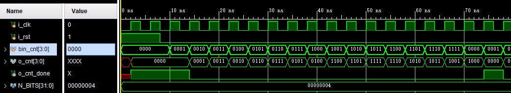
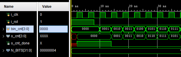
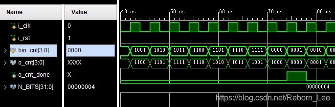
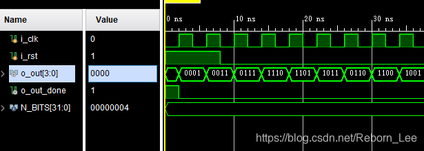
先假设定义了宏GRAY,仿真程序通用,如下:
`timescale 1ns/1ps
module sim_versatile_counter;

	parameter N_BITS = 4;
	reg i_clk;
	reg i_rst;
	wire [N_BITS - 1 : 0] o_out;
	wire o_out_done;

	initial begin
		i_clk = 0;
		forever begin # 2 i_clk = ~ i_clk;
		end
	end

	initial begin
		i_rst = 1; # 8
		i_rst = 0;

	end

	versatile_counter #(.N_BITS(N_BITS))
	inst_vc(
		.i_rst(i_rst),
		.i_clk(i_clk),
		.o_out(o_out),
		.o_out_done(o_out_done)
		);
endmodule
- 1
- 2
- 3
- 4
- 5
- 6
- 7
- 8
- 9
- 10
- 11
- 12
- 13
- 14
- 15
- 16
- 17
- 18
- 19
- 20
- 21
- 22
- 23
- 24
- 25
- 26
- 27
- 28
- 29
- 30
- 31
- 32
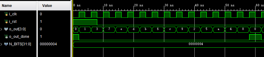
仿真波形 :
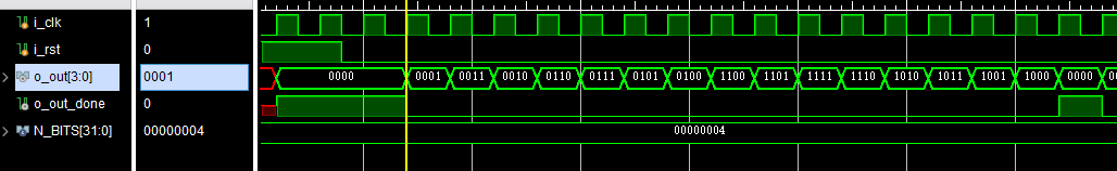
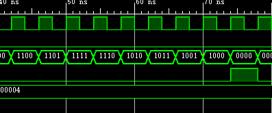
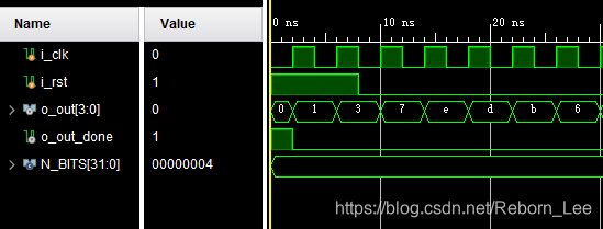
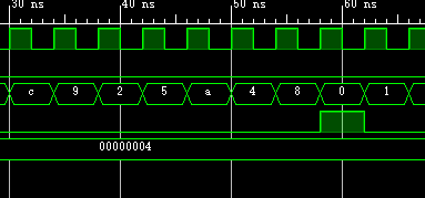
确实是格雷码计数器 ,放大:

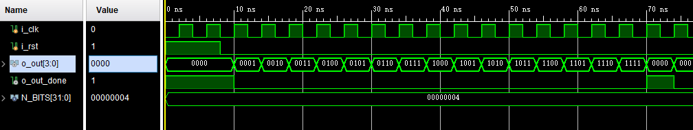
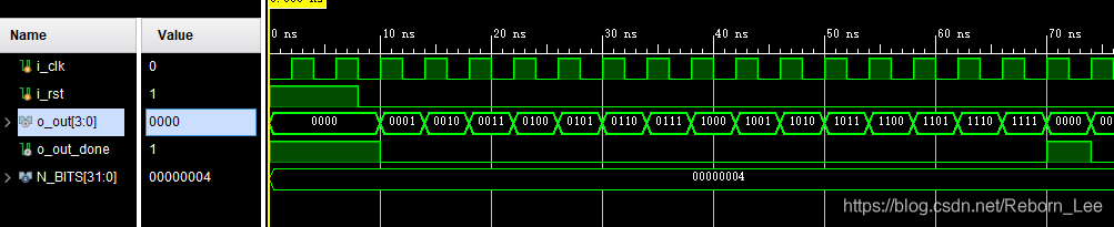
如果定义了宏BIN,
// `define LFSR_MACRO
// `define GRAY
`define BIN
- 1
- 2
- 3
则仿真图如下:
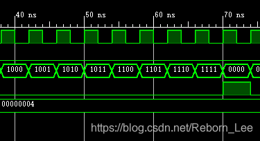
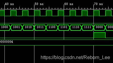
放大观测:

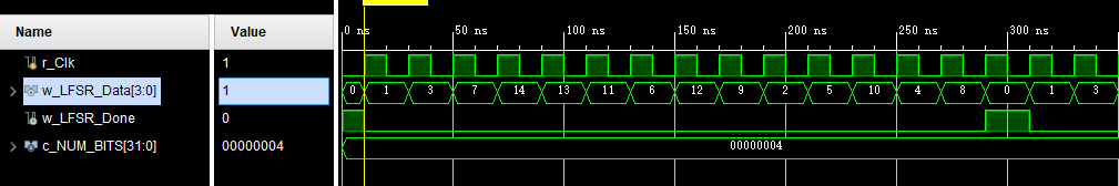
如果定义了宏LFSR_MACRO,则输出LFSR计数:
 `define LFSR_MACRO
// `define GRAY
//`define BIN
- 1
- 2
- 3


生成语句实现方式
这里使用生成语句,generate case来实现多功能计数器,我们需要定义一个参数SEL,当SEL为0的时候,输出为LFSR;当SEL为1时,输出为格雷码计数器;当SEL为2时候,输出为二进制计数器。
电路设计
`timescale 1ns / 1ps
//
// Create Date: 2020/06/02 16:22:52
// Design Name:
// Module Name: versatile_counter
// Revision 0.01 - File Created
// Additional Comments:
// Reborn Lee
//
module versatile_counter #(
	parameter N_BITS = 4,
	parameter SEL = 0

	)(
	input i_clk,
	input i_rst,
	output [N_BITS - 1 : 0] o_out,
	output o_out_done );


generate

	case(SEL) 0: begin lfsr #(.NUM_BITS(N_BITS)) LFSR_inst (.i_Clk(i_clk), .i_Enable(1'b1), .i_Seed_DV(1'b0), .i_Seed_Data({N_BITS{1'b0}}), // Replication .o_LFSR_Data(o_out), .o_LFSR_Done(o_out_done) );
		end
		1: begin gray_counter #(.N_BITS(N_BITS))
		inst_gray_cnt(
		.i_rst(i_rst),
		.i_clk(i_clk),
		.o_cnt(o_out),
		.o_cnt_done(o_out_done)
		);
		end
		2: begin binary_counter #(.N_BITS(N_BITS))
		inst_bin_cnt(
		.i_rst(i_rst),
		.i_clk(i_clk),
		.o_cnt(o_out),
		.o_cnt_done(o_out_done)
		); end endcase

endgenerate endmodule
- 1
- 2
- 3
- 4
- 5
- 6
- 7
- 8
- 9
- 10
- 11
- 12
- 13
- 14
- 15
- 16
- 17
- 18
- 19
- 20
- 21
- 22
- 23
- 24
- 25
- 26
- 27
- 28
- 29
- 30
- 31
- 32
- 33
- 34
- 35
- 36
- 37
- 38
- 39
- 40
- 41
- 42
- 43
- 44
- 45
- 46
- 47
- 48
- 49
- 50
- 51
- 52
- 53
- 54
- 55
- 56
- 57
- 58
- 59
- 60
- 61
- 62
- 63
- 64
- 65
行为仿真
SEL为0,也即LFSR:
仿真文件例化改为:
	versatile_counter #(
		.N_BITS(N_BITS),
		.SEL(0)
		)
	inst_vc(
		.i_rst(i_rst),
		.i_clk(i_clk),
		.o_out(o_out),
		.o_out_done(o_out_done)
		);
- 1
- 2
- 3
- 4
- 5
- 6
- 7
- 8
- 9
- 10
放大:
SEL为1,也即格雷码计数器:
仿真文件例化改为:
	versatile_counter #(
		.N_BITS(N_BITS),
		.SEL(1)
		)
	inst_vc(
		.i_rst(i_rst),
		.i_clk(i_clk),
		.o_out(o_out),
		.o_out_done(o_out_done)
		);
- 1
- 2
- 3
- 4
- 5
- 6
- 7
- 8
- 9
- 10

放大:


SEL为2,也即 二进制计数器:
仿真文件例化改为:
	versatile_counter #(
		.N_BITS(N_BITS),
		.SEL(2)
		)
	inst_vc(
		.i_rst(i_rst),
		.i_clk(i_clk),
		.o_out(o_out),
		.o_out_done(o_out_done)
		);
- 1
- 2
- 3
- 4
- 5
- 6
- 7
- 8
- 9
- 10
放大:

注意事项
关于多功能计数器的注意事项,这里不做多说,
在debug的过程中,可以先进行elaborated design,
如果没有错误,在进行行为仿真;
其次需要注意,在宏定义过程中,别忘了`这个符号。
就这样吧,感觉如此实现也不是太难,我还记得使用OPENCORES里的那个设计实例,编译预处理指令一大堆,看得我头皮发麻,最关键的是我还没编译通过。
工程要不要分享了呢?暂时算了吧,反正代码已经贴出来了,实在需要的可以说一声。
工具 :vivado 2019.1
参考资料
交个朋友
文章来源: reborn.blog.csdn.net,作者:李锐博恩,版权归原作者所有,如需转载,请联系作者。
原文链接:reborn.blog.csdn.net/article/details/106498495

- 点赞
- 收藏
- 关注作者
评论(0)